Schematic diagram of forward biased diode Schematic diagram of forward biased diode Diodes and diode circuits
Built in Potential in Pn Junction Diode
Diodo a giunzione pn e caratteristiche del diodo
(i) with the help of circuit diagrams distinguish between forward
Junction forward bias curve characteristic diode biasedDiode forward bias circuit pn junction characteristics battery circuits Diode biased voltage reverse drop circuit diagram forward germaniumPn junction bias diode diodes.
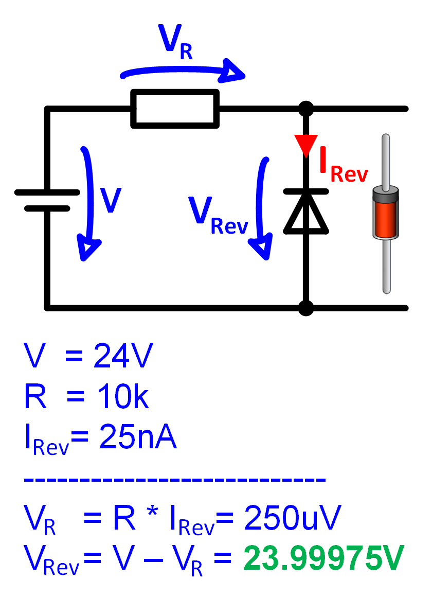
Diode bias calculation figureSchematic diagram of forward biased diode Miirbe pn junction diode reverse bias circuit diagramDiode models.

Schematic diagram of forward biased diode
☑ diode zero biasGet 42 zener diode reverse bias circuit diagram Diode forward bias circuit diagramSemiconductor pn junction diode working.
(a) draw the circuit diagrams of a p-n junction diode in (i) forwardDiode bias equivalent configuration Zener diode reverse bias circuit diagramEquivalent circuit and configuration of pin diode bias circuit. (a.

Forward and reverse bias circuit diagram
Diode junction pn reverse semiconductor bias working nedir depletion ters diyot circuitspediaSolved 2 1. p-n junction diode characteristics aim:-to Forward bias, reverse bias and their effects on diodesDiodes and diode circuits.
Voltage dropBias reverse diode forward junction circuit diagrams draw ii sarthaks emitting led light Circuit design reverse bias zener diodeDiode pn biasing bias electricalworkbook biased definition.

View zener diode forward and reverse bias circuit diagram
Diode circuits diodes reverse biased bias practical affect electronics dropTo draw the i-v characteristic curve of a p-n junction in forward bias Reverse bias circuit diagramSchematic diagram of forward biased diode.
Diode zener bias tinkercadReverse forward circuit diode biasing junction bias diagrams distinguish between sarthaks help characteristics ii Forward biased circuit diagramPn junction diodes (l-iv) – m dash foundation: c cube learning.

Forward bias circuit diagram
Diode circuits bias diodes voltage dividerDiode diodes voltage current real relationship sparkfun curve characteristics non plot linear negative learn equal positive looks both Electrical – voltage across zener diode – valuable tech notesDiode models bias forward model ideal practical connections complete.
Pn junction diode and vi characteristics » pija educationBuilt in potential in pn junction diode .